- 您现在的位置:买卖IC网 > Sheet目录2006 > LTC2305CDE#TRPBF (Linear Technology)IC ADC 12-BIT 2CHN 12-DFN
LTC2301/LTC2305
5
23015fb
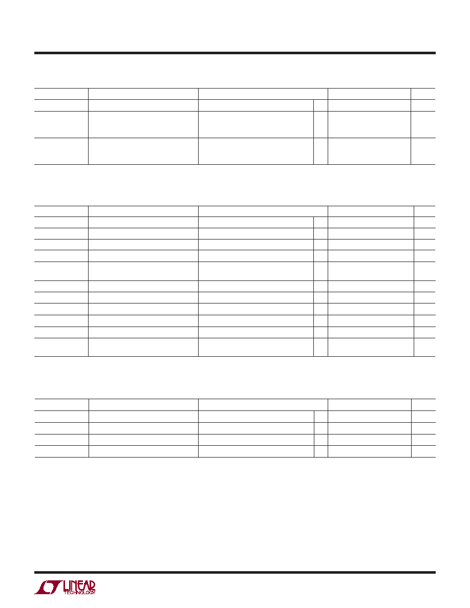
POWER REQUIREMENTS
SYMBOL
PARAMETER
CONDITIONS
MIN
TYP
MAX
UNITS
VDD
Supply Voltage
l
4.75
5
5.25
V
IDD
Supply Current
Nap Mode
Sleep Mode
14ksps Sample Rate
SLP Bit = 0, Conversion Done
SLP Bit = 1, Conversion Done
l
2.3
225
7
3.5
400
15
mA
μA
PD
Power Dissipation
Nap Mode
Sleep Mode
14ksps Sample Rate
SLP Bit = 0, Conversion Done
SLP Bit = 1, Conversion Done
l
11.5
1.125
35
17.5
2
75
mW
μW
The
l denotes the specications which apply over the full operating temperature
range, otherwise specications are at TA = 25°C. (Note 4)
I2C TIMING CHARACTERISTICS
SYMBOL
PARAMETER
CONDITIONS
MIN
TYP
MAX
UNITS
fSCL
SCL Clock Frequency
l
400
kHz
tHD(SDA)
Hold Time (Repeated) START Condition
l
0.6
μs
tLOW
LOW Period of the SCL Pin
l
1.3
μs
tHIGH
HIGH Period of the SCL Pin
l
0.6
μs
tSU(STA)
Set-Up Time for a Repeated START
Condition
l
0.6
μs
tHD(DAT)
Data Hold Time
l
0
0.9
μs
tSU(DAT)
Data Set-Up Time
l
100
ns
tr
Rise Time for SDA/SCL Signals
(Note 11)
l
20 + 0.1CB
300
ns
tf
Fall Time for SDA/SCL Signals
(Note 11)
l
20 + 0.1CB
300
ns
tSU(STO)
Set-Up Time for STOP Condition
l
0.6
μs
tBUF
Bus Free Time Between a Second START
Condition
l
1.3
μs
The
l denotes the specications which apply over the full operating
temperature range, otherwise specications are at TA = 25°C. (Note 4)
ADC TIMING CHARACTERISTICS The l denotes the specications which apply over the full operating
temperature range, otherwise specications are at TA = 25°C. (Note 4)
SYMBOL
PARAMETER
CONDITIONS
MIN
TYP
MAX
UNITS
fSMPL
Throughput Rate (Successive Reads)
l
14
ksps
tCONV
Conversion Time
l
1.3
1.6
μs
tACQ
Acquisition Time
(Note 8)
l
240
ns
tREFWAKE
REFCOMP Wakeup Time (Note 12)
CREFCOMP = 10μF, CREF = 2.2μF
200
ms
发布紧急采购,3分钟左右您将得到回复。
相关PDF资料
LTC2306CDD#PBF
IC ADC 12BIT 2CH 500KSPS 10-DFN
LTC2351HUH-12#TRPBF
IC ADC 12BIT 1.5MSPS 32-QFN
LTC2351HUH-14#TRPBF
IC ADC 14BIT 1.5MSPS 32-QFN
LTC2355IMSE-14#TRPBF
IC ADC 14BIT 3.5MSPS 10-MSOP
LTC2356IMSE-14#TRPBF
IC ADC 14BIT 3.5MSPS 10-MSOP
LTC2366HTS8#TRPBF
IC ADC 12BIT 3MSPS TSOT23-8
LTC2379HMS-18#PBF
IC ADC 18BIT SPI/SRL 16MSOP
LTC2380HMS-16#TRPBF
IC ADC 16BIT 2MSPS 16-MSOP
相关代理商/技术参数
LTC2305CMS#PBF
功能描述:IC ADC 12-BIT 2CHN 12-MSOP RoHS:是 类别:集成电路 (IC) >> 数据采集 - 模数转换器 系列:- 标准包装:2,500 系列:- 位数:16 采样率(每秒):15 数据接口:MICROWIRE?,串行,SPI? 转换器数目:1 功率耗散(最大):480µW 电压电源:单电源 工作温度:-40°C ~ 85°C 安装类型:表面贴装 封装/外壳:38-WFQFN 裸露焊盘 供应商设备封装:38-QFN(5x7) 包装:带卷 (TR) 输入数目和类型:16 个单端,双极;8 个差分,双极 配用:DC1011A-C-ND - BOARD DELTA SIGMA ADC LTC2494
LTC2305CMS#PBF
制造商:Linear Technology 功能描述:ADC, 12BIT, 14KSPS, MSOP-12
LTC2305CMS#TRPBF
功能描述:IC ADC 12-BIT 2CHN 12-MSOP RoHS:是 类别:集成电路 (IC) >> 数据采集 - 模数转换器 系列:- 标准包装:2,500 系列:- 位数:16 采样率(每秒):15 数据接口:MICROWIRE?,串行,SPI? 转换器数目:1 功率耗散(最大):480µW 电压电源:单电源 工作温度:-40°C ~ 85°C 安装类型:表面贴装 封装/外壳:38-WFQFN 裸露焊盘 供应商设备封装:38-QFN(5x7) 包装:带卷 (TR) 输入数目和类型:16 个单端,双极;8 个差分,双极 配用:DC1011A-C-ND - BOARD DELTA SIGMA ADC LTC2494
LTC2305HMS#PBF
功能描述:IC ADC 12-BIT 2CHN 12-MSOP RoHS:是 类别:集成电路 (IC) >> 数据采集 - 模数转换器 系列:- 标准包装:2,500 系列:- 位数:16 采样率(每秒):15 数据接口:MICROWIRE?,串行,SPI? 转换器数目:1 功率耗散(最大):480µW 电压电源:单电源 工作温度:-40°C ~ 85°C 安装类型:表面贴装 封装/外壳:38-WFQFN 裸露焊盘 供应商设备封装:38-QFN(5x7) 包装:带卷 (TR) 输入数目和类型:16 个单端,双极;8 个差分,双极 配用:DC1011A-C-ND - BOARD DELTA SIGMA ADC LTC2494
LTC2305HMS#TRPBF
功能描述:IC ADC 12-BIT 2CHN 12-MSOP RoHS:是 类别:集成电路 (IC) >> 数据采集 - 模数转换器 系列:- 标准包装:2,500 系列:- 位数:16 采样率(每秒):15 数据接口:MICROWIRE?,串行,SPI? 转换器数目:1 功率耗散(最大):480µW 电压电源:单电源 工作温度:-40°C ~ 85°C 安装类型:表面贴装 封装/外壳:38-WFQFN 裸露焊盘 供应商设备封装:38-QFN(5x7) 包装:带卷 (TR) 输入数目和类型:16 个单端,双极;8 个差分,双极 配用:DC1011A-C-ND - BOARD DELTA SIGMA ADC LTC2494
LTC2305IDE#PBF
功能描述:IC ADC 12-BIT 2CHN 12-DFN RoHS:是 类别:集成电路 (IC) >> 数据采集 - 模数转换器 系列:- 标准包装:2,500 系列:- 位数:16 采样率(每秒):15 数据接口:MICROWIRE?,串行,SPI? 转换器数目:1 功率耗散(最大):480µW 电压电源:单电源 工作温度:-40°C ~ 85°C 安装类型:表面贴装 封装/外壳:38-WFQFN 裸露焊盘 供应商设备封装:38-QFN(5x7) 包装:带卷 (TR) 输入数目和类型:16 个单端,双极;8 个差分,双极 配用:DC1011A-C-ND - BOARD DELTA SIGMA ADC LTC2494
LTC2305IDE#TRPBF
功能描述:IC ADC 12-BIT 2CHN 12-DFN RoHS:是 类别:集成电路 (IC) >> 数据采集 - 模数转换器 系列:- 标准包装:2,500 系列:- 位数:16 采样率(每秒):15 数据接口:MICROWIRE?,串行,SPI? 转换器数目:1 功率耗散(最大):480µW 电压电源:单电源 工作温度:-40°C ~ 85°C 安装类型:表面贴装 封装/外壳:38-WFQFN 裸露焊盘 供应商设备封装:38-QFN(5x7) 包装:带卷 (TR) 输入数目和类型:16 个单端,双极;8 个差分,双极 配用:DC1011A-C-ND - BOARD DELTA SIGMA ADC LTC2494
LTC2305IMS#PBF
功能描述:IC ADC 12BIT I2C 12-MSOP RoHS:是 类别:集成电路 (IC) >> 数据采集 - 模数转换器 系列:- 标准包装:1 系列:microPOWER™ 位数:8 采样率(每秒):1M 数据接口:串行,SPI? 转换器数目:1 功率耗散(最大):- 电压电源:模拟和数字 工作温度:-40°C ~ 125°C 安装类型:表面贴装 封装/外壳:24-VFQFN 裸露焊盘 供应商设备封装:24-VQFN 裸露焊盘(4x4) 包装:Digi-Reel® 输入数目和类型:8 个单端,单极 产品目录页面:892 (CN2011-ZH PDF) 其它名称:296-25851-6